EE1C2 Assignment
by: Joost Koch 2025
(simulations) EE1L11 LTSpice Tue week 2.1121.pdf
📌 Overview
Learning to use LTspice to create and simulate diagrams and test hypotheses about circuits
Assignment 1
- Calculate the value of the resonant frequency 𝜔0 (rad/s) and 𝑓0 (Hz).
- Calculate the value for the resistance R where the damping factor (α) is equal to 𝜔0 (rad/s).
- Calculate the value for the resistance R where the damping factor (α) is equal to 0.25*𝜔0 (rad/s).
- Calculate the value for the resistance R where the damping factor (α) is equal to 5*𝜔0 (rad/s).
- Obtain the simulation result for the voltage across the capacitor using the value of R where the damping factor (α) is equal to 𝜔0 (rad/s). See above
- Obtain the simulation result for the voltage across the capacitor using the value of R where the damping factor (α) is equal to 0.25*𝜔0 (rad/s). See above
- Obtain the simulation result for the voltage across the capacitor using the value of R where the damping factor (α) is equal to 5*𝜔0 (rad/s). See above
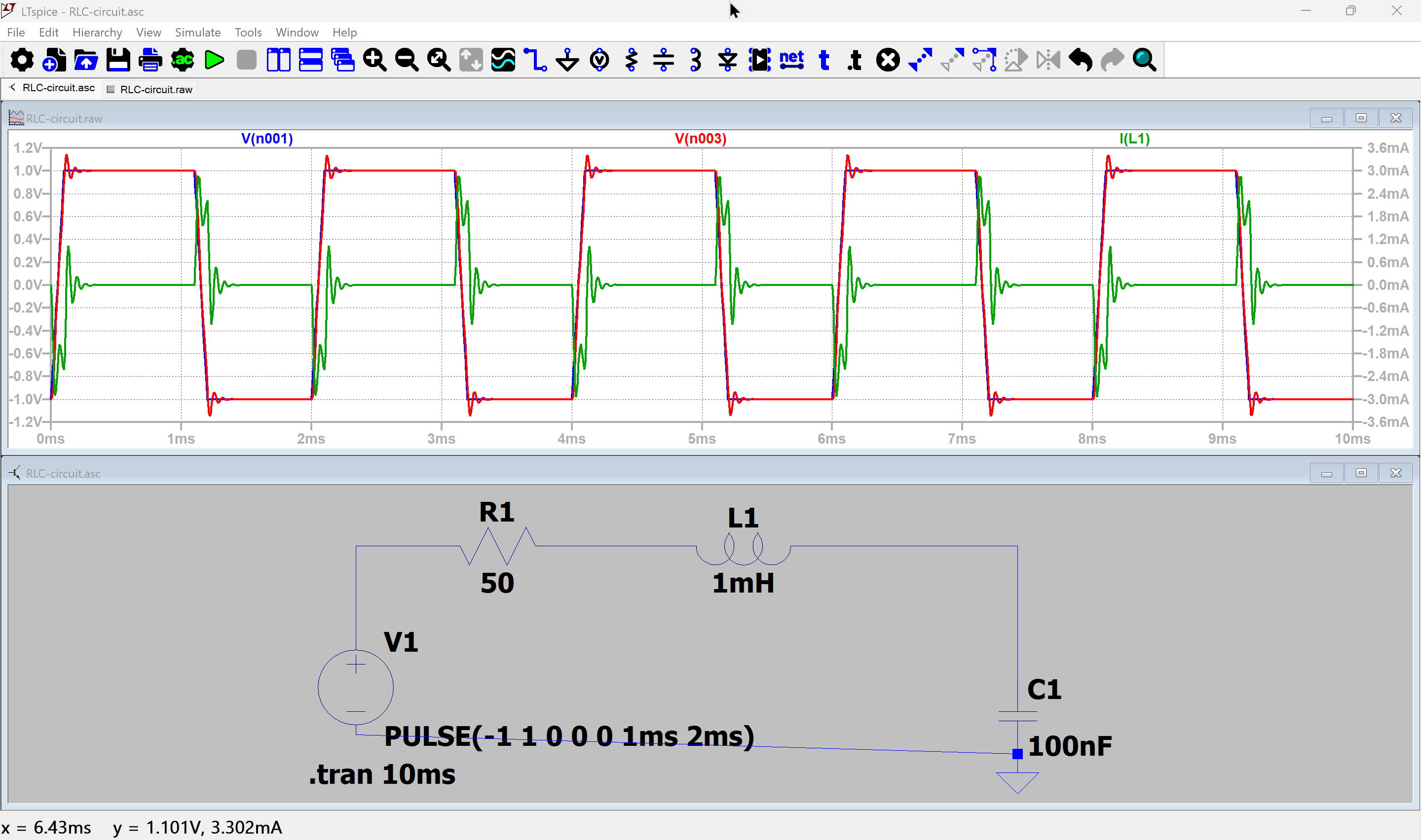
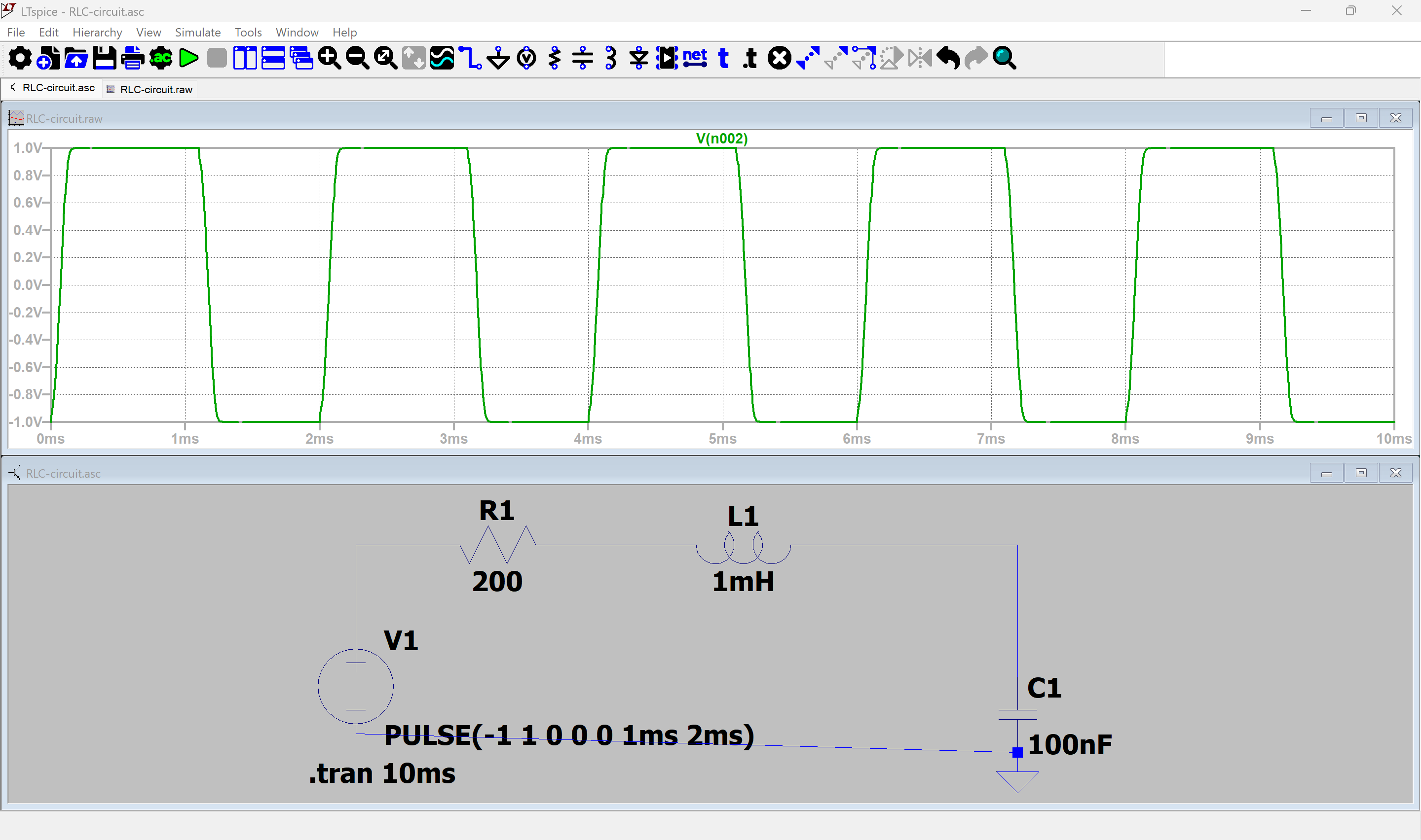
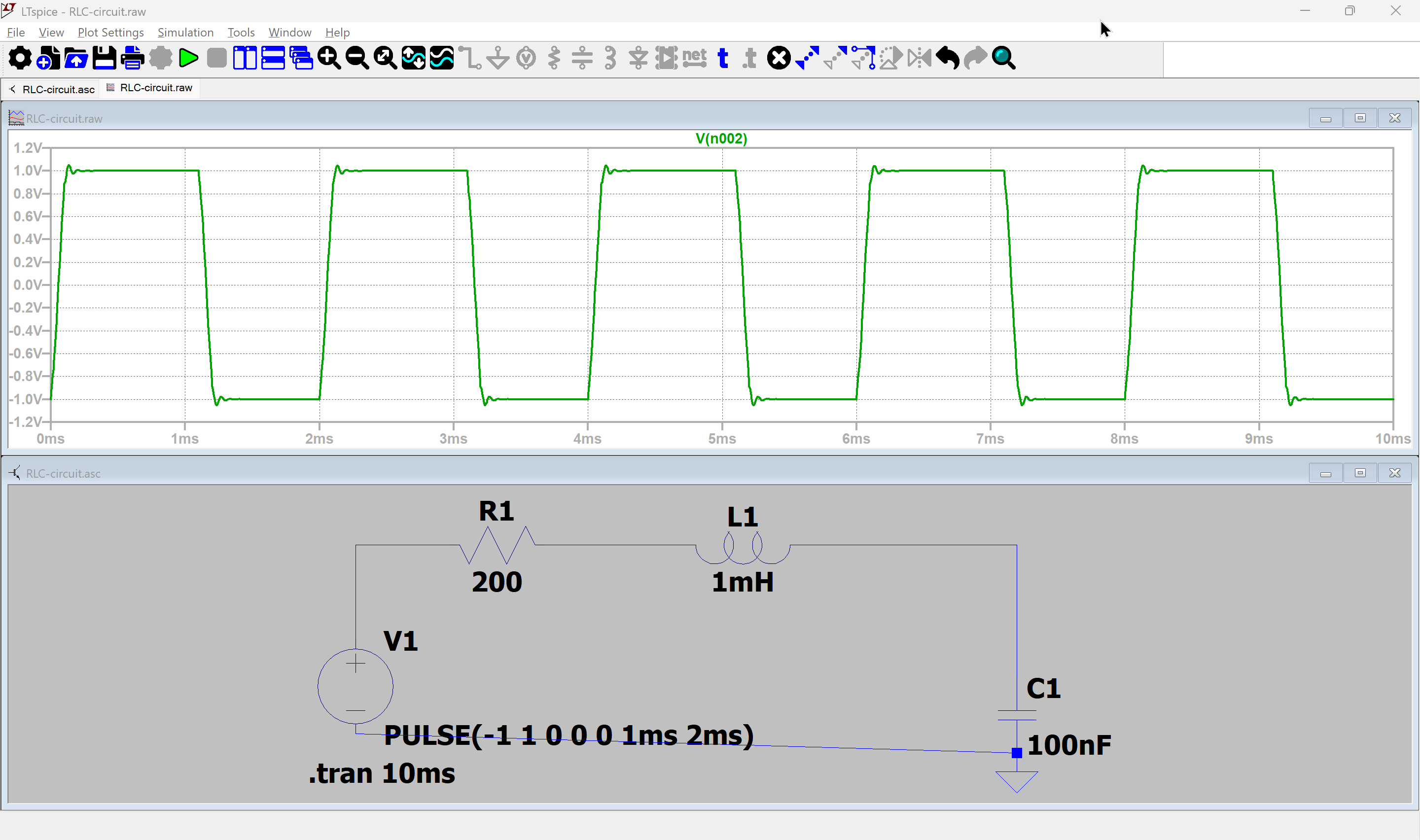
- Compare your simulation results for the previous three cases with three different values for R (overdamped, underdamped and critically damped). The simulation results visually confirm the calculated conditions for damping. The circuit with R = 200 Ω exhibits a critically damped response, settling quickly without oscillation, while the R = 50 Ω circuit shows the oscillatory behavior of an underdamped system. Conversely, the R = 1000 Ω circuit demonstrates a slow, non-oscillatory response characteristic of an overdamped system, aligning perfectly with the theoretical predictions.
- For the underdamped case, obtain the value of the damped natural frequency 𝜔𝑑. Then, give the damped natural frequency from your simulation results. Does the damped natural frequency from your simulation results match the calculated value?
From the simulation graph for R = 50 Ω, .
The minor difference is attributable to measurement inaccuracies from the plot.
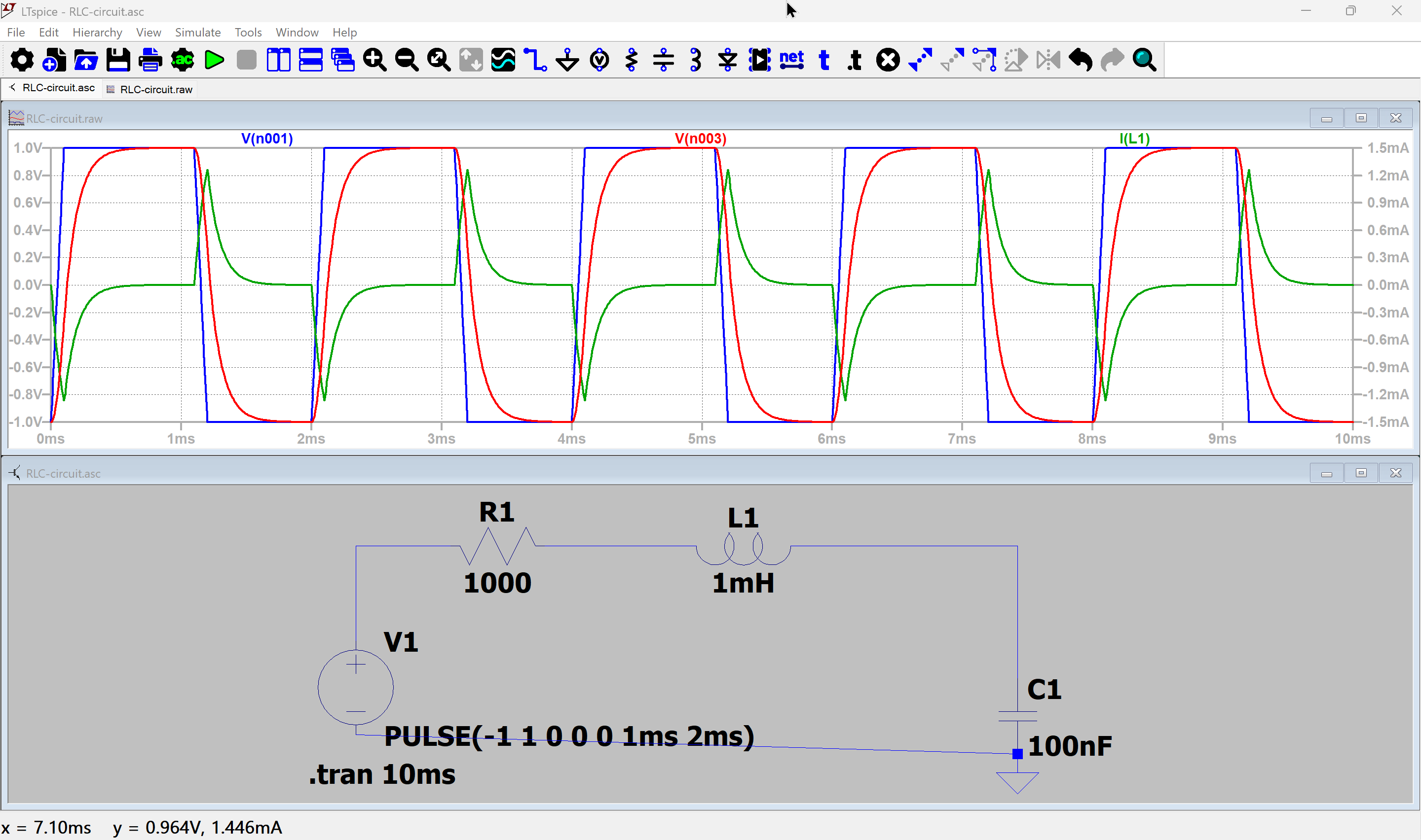
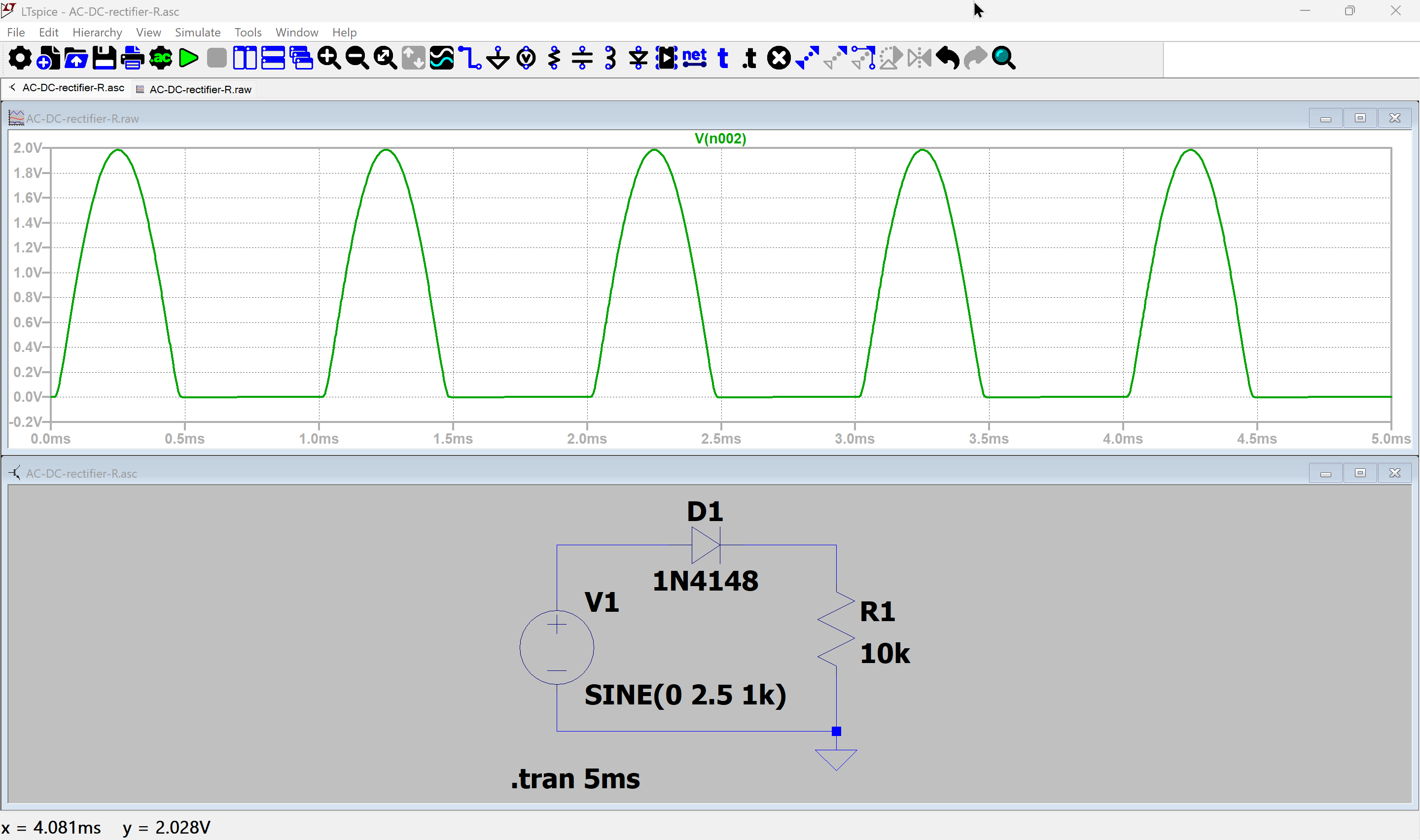
Assignment 2
- Obtain the simulation results for 𝑉𝑅 in the circuit shown in Fig. 2. Does the simulation result match your drawings? Yes only the positive sinusoids go through the diode and the voltage is reduces by .5V because of the diodes voltage drop
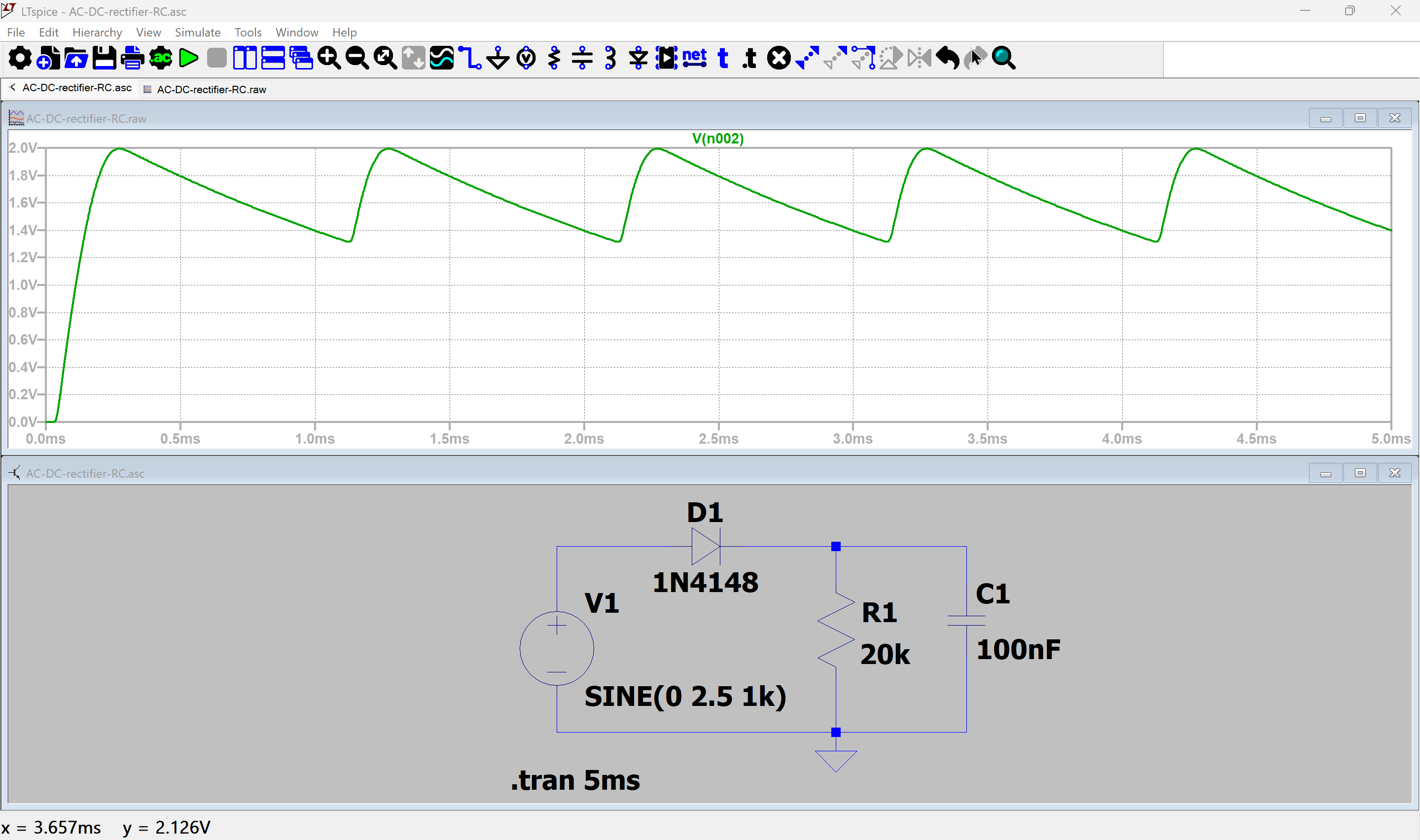
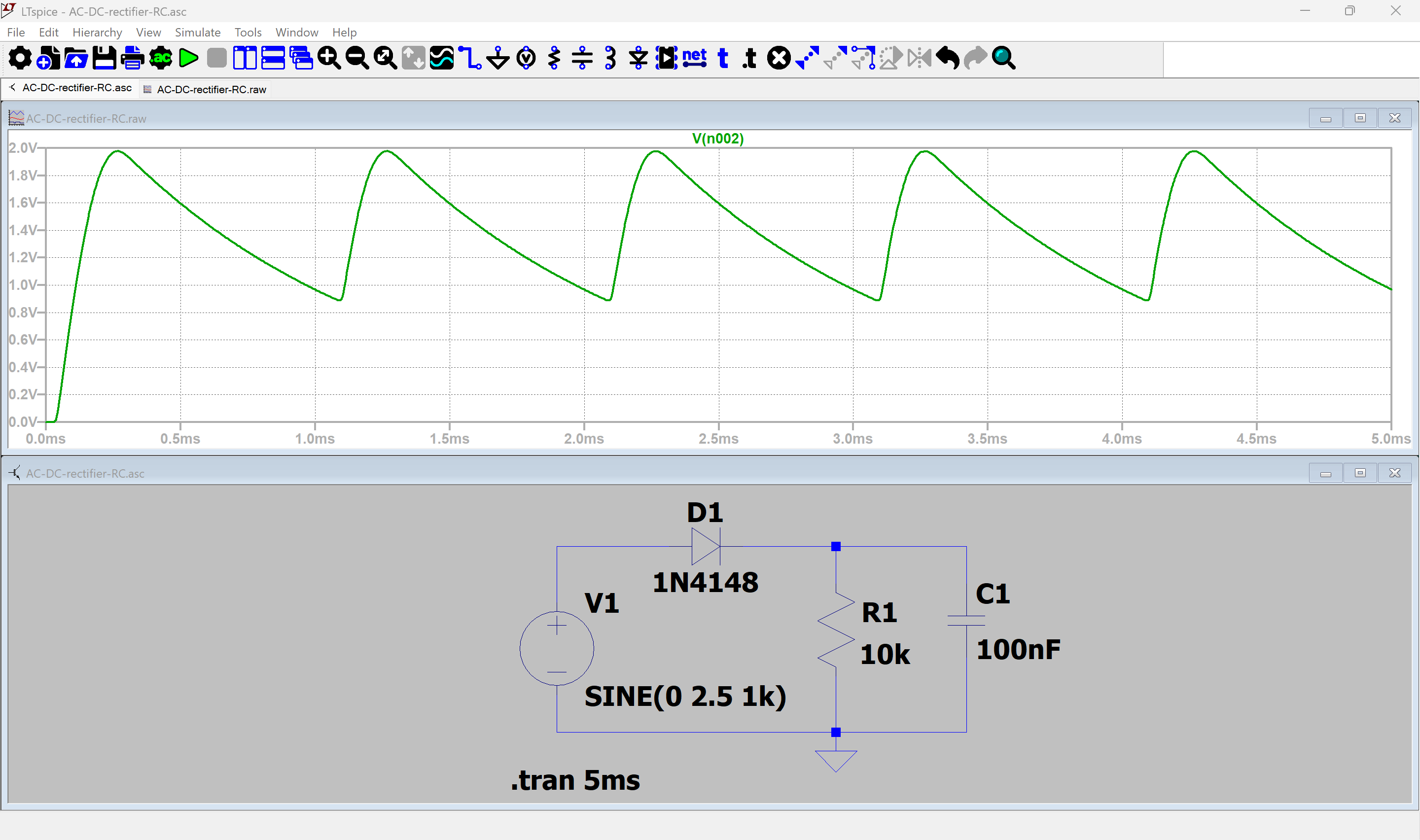
- Obtain the simulation results for 𝑉𝑅C in the circuit shown in Fig. 3. What is the impact of the capacitor on the output DC voltage?
It smooths out the drop of the voltage, because no current can flow back through the diode the capacitor can slowly release the voltage through the resistor
- Repeat the simulations where you use a 20 KΩ resistor (instead of a 10 KΩ resistor). What is the impact of the value of the resistance on the output DC voltage?
The voltage voltage drops slower on the negative cycle of the source’s period
because the resistor is resisting the current flow more so the capacitor can drop it’s voltage less fast